Large-Signal Approach Yields Low-Noise VHF/UHF Oscillators
Incontrast to traditional small-signal approaches, the use of large-signal, time-domain design techniques helps deliver low-noise grounded-base oscillators for VHF/UHF applications.
Oscillator design for veryhigh-frequency (VHF) and ultra-high-frequency(UHF) applications has been well documented inbooks and journals. Most early work focused on frequency stability and, to a lesser extent, on efficiency and output signal quality. But with increasing use of advanced modulation formatsin communications systems, and the growing need for oscillators with extremely lowphase noise, greater design emphasis is now placed onachieving oscillator designs with low phase noise. Fortunately, with the availability of accurate phase-noise measurement equipment and improving computer-aided engineering (CAE) tools for predicting and simulating phase-noise performance, the gap between oscillator simulationsand measured results has narrowed. Still, many early oscillator design strategies were based on small-signal approaches that yielded less-than-accurate predictions for output frequency, output power, andphase noise. As an alternative, largesignal, time-domain calculations willbe applied to the design of a grounded base oscillator (rather than a Colpitts oscillator) to validate the effectiveness of this design approach. Part 1 of thisthree-part article series will explore the use of large-signal design techniques for a grounded-base 144-MHz oscillator.
By presenting the use of the large signal, time-domain approach with nonlinear software simulation tools in the design of VHF/UHF grounded based oscillators, the goals include (1) accurately predicting oscillator phase noise and deriving a set of algebraic equations for the noise calculations (many CAE tools provide incorrect answers about the phase noise) and (2) developing a set of empirical equations that will guide in the synthesis of VHF/UHF oscillators. The approach yields oscillators with the best possible combination of output power and phase noise.
As a point of reference, the traditional small-signal design approach will first be used to create an oscillator for comparison to a more optimized design developed with the novel large-signal approach. Using a mix of linear equations and one large signal parameter, the device transconductance (gm), the important noise parameters will be calculated and validated. Finally, based on this procedure, a simple but scalable and accurate set of formulas for oscillator synthesis will be presented. The novel large-signal design principles shown here for fixed or narrowband oscillators can also be applied to broadband voltage-controlled-oscillator (VCO) design. The methodology has been shown to work well even with multi-octave-band (1:3 frequency tuning range) tunable oscillators.20-32
The grounded base configuration (Fig. 1) is a popular circuit for VHF/UHF oscillators. It is simple and can be made with very low phase noise, since the RF voltage swing at the active-device's collector can be close to that of the supply voltage. Oscillation is based on the principle that power from the output is fed back to the emitter. This feedback arrangement generates a negative resistance at the output, compensating for the losses of the output-tuned circuit, and starts oscillating and then stabilizing the oscillation amplitude.1-4 A complete survey of grounded-base oscillator configurations and applications can be found in references 5 to 19.
These references include some of the more popular texts recently published on oscillators. Many of the authors have attempted to predict oscillator performance based on a set of linear calculations, including use of the Leeson model or similar methods to determine phase noise. For accurate predictions of phase noise, however, several key input parameters are needed, including the large-signal noise figure of the active device, the output power, and the operating quality factor (Q). The values of these parameters are not often known and more typically approximated (or guessed). The first successful attempts at determining the large-signal phase noise were reported in references 6 and 7. But these approaches are not useful without an accompanying CAE tool, and they don't provide design guidelines. Another problem with the linear approach is inaccuracy in predicting the actual oscillating frequency, with predicted results at higher frequencies often differing widely from actual performance.
Well-known for his work on amplifiers, Guillermo Gonzalez recently published a text on oscillators that provides an interesting overview of design based on linear calculations and CAE tools, although his approach does not provide optimum solutions. To demonstrate this, his methods will first be applied to the design of a 144-MHz oscillator. The resulting circuit neither provides the best output power nor the lowest phase noise and, at high frequencies, requires capacitor values that cannot be easily realized because of parasitic effects.
Figure 1 shows the typical configuration of the grounded base oscillator circuit. This type of oscillator works effectively from about 10 to above 1000 MHz. Following the procedures of ref. 8, and the large-signal conditions of ref. 11, it is possible to analyze this oscillator circuit. Kenneth Clarke was probably the first to publish the effect of the collector current conducting angle of an oscillator, but makesno mention of the relationship of it on phase noise, as done in ref. 10.
The oscillator circuit is based on a model BFR193 silicon bipolar transistor from Infineon Technologies (www.infineon.com). Designed for low-noise, high-gain amplifiers to 2 GHz, the transistor features a transition frequency (fT) of 8 GHz for +8 VDC collectoremitter voltage and 50 mA collector current. The first step in designing the oscillator circuit for this transistor is to determine the small-signal [Y] parameters for the transistor at 144 MHz and under the operating conditions of +8.8 VDC collector-emitter voltage (Vce, 10 mA collector current (Ic), 24 µA base current (IB), and +0.64 VDC base-emitter voltage (Vbe). The 10-mA collector current was selected for stable transistor cut-off transition frequency. For more output power, a collector current of 30 mA is a better choice.
Figure 2 shows a circuit for generating the oscillator’s small-signal [Y] parameters using Ansoft Designer CAE software from Ansoft (www.ansoft.com) and the time-domain model. The process is based on the configuration shown in Fig. 3 and the following definition:
[ |
I1 |
]
|
[ |
Y11 |
Y12 |
] | [ |
V1 |
] |
(1) |
|
I2 |
Y21 |
Y22 |
V2 |
Once Ansoft Designer is armed with the circuit parameters for the oscillator circuit, it uses the [Y] matrix to generate the Y-parameters:
Y11=G11 + jB11= (279.08-j95.07mS (2)
Y21=G21 + jB21= (-271.32 + j100.77)mS (3)
Y12=G12 + jB12= (-1030 + j78.06) μS (4)
Y22=G22 + jB22= (1020 + j536.14) μS (5)
Figure 4 shows a standard feedback oscillator topology using parallel circuit elements. In theory, the grounded-base configuration can be rotated into a Colpitts circuit, which is often referenced in the technical literature and based on the black-box theory (ref. 5). In terms of performance, however, it cannot be said that a mathematical rotation yields the same performance. In the case of the Colpitts oscillator, the RF voltage swing is now limited by the base-to-emitter and emitter-to-ground voltages. As a result, there is less energy stored in the circuit and, because of loading, the operational Q can be degraded for the grounded-base oscillator. For the Colpitts oscillator configuration, the collector-to-base voltage (Vcb) is about 12 V. Also, parameter Y22cb is less than parameter Y22ce, resulting in less loading than the grounded-base configuration. The Colpitts configuration is popular because of its simplicity and its perceived high isolation since the output power is extracted from the collector, although this is nothing more than perception due to the strong Miller effect at very high frequencies. In terms of configurations other than the Colpitts, the general time-domain approach presented here is valid not only for the Colpitts configuration but for other derivative configurations.
Conditions necessary for oscillation for the parallel feedback oscillator configuration of Fig. 4 can be described by
Yout + Y3 =>0 (6)
This condition can be expressed as:
Det |
[ |
Y11 + Y1 + Y2 Y12-Y2 |
] | =0 | (7) |
Y21-Y2 Y22 + Y2 + Y3 |
| Y3= -[Y22+Y2] + | [Y12-Y2{Y21-Y2} |
(8) |
[Y11 + Y1 + Y2] |
where Yij (i,j = 1, 2) are the smallsignal [Y] parameters of the bipolar or FET model.
As shown in Fig. 4, the active two-port network, together with feedback elements Y1 and Y2, can be considered as a one-port negative-resistance oscillator circuit. The following is an example of an oscillator design using the small-signal parameters determined above for 8.8 V and 10 mA at 144 MHz. The resulting output admittance (Yout) is shown in Eq. 9 (page 76).
The optimum values of feedback element are calculated from the expression of B*1 and B*2 and for 10 mA are shown in Eq. 10 (page 76).

(10 x 47 pF in parallel)

The optimum values of the real and imaginary part of the output admittance are:
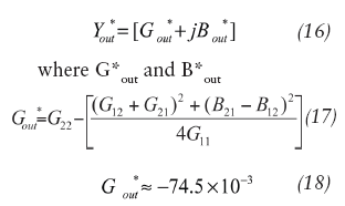
are values for conjugate matching needed to compensate for resonator losses in Eq. 19 (on p. 76) and in:
for the case of a center frequency (f0 of 144 MHz and inductor L3 of approximately 2.59 nH).
Figure 5 shows the 144-MHz oscillator circuit using the small-signal [Y] parameters for establishing oscillation conditions. The required values for this parallel feedback topology are 478 pF for the feedback capacitor, 459 pF for the emitter-to-ground capacitance, 3.2 nH for the inductor, and 186 pF for capacitors C3A and C3B. Bypass capacitors Cb and Cc should be about 220 pF. Because of the difficulty of producing capacitors above 200 pF at these frequencies, it may be more reasonable to use several, up to 10, capacitors in parallel to achieve these values.
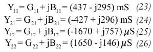
For the higher-output oscillator case operating at 30 mA, the values of the [Y] parameters are:

For a center frequency (f0) of 144 MHz and 30 mA operation, the component values for the oscillator are L3 of 3.77 nH, C1 of 518 pF, C2 of 503 pF, and C3 of 324 pF. As mentioned previously, because of the high values of C1 and C2, their values can only be achieved using multiple parallel capacitors of about 100 pF each.
Figure 6 shows the simulated plot of phase noise for the 144-MHz oscillator. The “linear” calculation indicates a resonant frequency of 143.2 MHz, while nonlinear harmonicbalance (HB) analysis provides the correct frequency of 144.2 MHz (a relatively large difference in percent frequency). Figure 7 shows the output power to be +5.1 dBm. The value was determined using the HB software program Nexxim from Ansoft Designer, although the Advanced Design System (ADS) software suite from Agilent Technologies (www.agilent.com) provided the same answers. The predictions from both CAE tools deviate less than 1 dB from measured results for the oscillator, assuming that the input SPICE type parameters for the transistor are accurate.
A variety of efforts have been made to deal with large-signal conditions for oscillator design, such as the time domain approach. Reference 10 is a first successful attempt to calculate output power with reasonable effort, notably Eq. 10 within this reference.
There are many problems associated with both the large-signal analysis and noise analysis. From an experimental point of view, it is almost impossible to consider all possible variations. During the creation of the Ansoft Designer CAE program, for example, it was necessary for the developers to validate the accuracy of that software’s large-signal noise analysis. As part of that validation, several critical circuits were used to compare CAE predictions with measured results, from crystal oscillators to voltage-controlled oscillators (VCOs). Measurements were made with well-known test equipment, including the R&S FSUP 26 spectrum analyzer with all necessary options from Rohde & Schwarz (www.rohdeschwarz.com). References 12 and 13 showed that the accuracy of this software's large-signal predictions is high, within 0.5 dB of measured results. This evaluation involved extensive analysis of noise in oscillators using a set of equations with a minimum number of CAE tools. The equations, derived in ref. 9, will be used for the current analysis.
The search for low oscillator phase noise has been well documented in the technical literature. Designers have published many different recipes, such as those based on the use of certain low-noise transistors, high-Q circuits, and various other things. In all of these approaches, however, the consequences of device large-signal operation and its effects on phase noise had not been well understood. To help gain a better grasp on the relationship between device large-signal behavior and phase noise, a complete mathematical analysis of a 144-MHz oscillator follows.
The design steps for achieving a 144-MHz oscillator by means of the large-signal approach include:
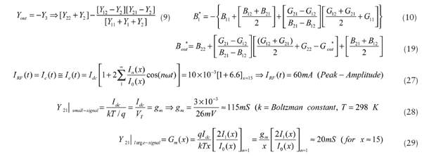
1. Calculation of the output power for the selected DC operating conditions. For this example, the same circuit as used above for the small-signal approach will be applied for a center frequency of 144 MHz. From ref. 9, the RF output current can be found from Eq. 27 (above) where:
V1 = the drive signal and x = the normalized drive level with x = qV1/kT with
Considering a 50-Ohm load, the RF output power can be calculated by means of
VRF(f0 = IRF × 50 = 60 × 10-3 × 50 = 1 V (peak amplitude) (with no Vce saturation assumed).
The oscillator output power at 144 MHz is then Pout(f0 = VRF2(f0/2RL = 1/(2 × 50) = 10 mW = +10 dBm
2. Calculation of the large-signal transconductance for a normalized drive level can be performed by means of Eq. 28 (above), while the largesignal transconductance (Gm) can be found from Eq. 29 (above).
This assumes an ideal intrinsic transistor. To perform the transition from an intrinsic to an extrinsic transistor, parasitics (package effects, lead inductance, and bond wires) are added by correcting the final results for capacitances and inductances. The transition frequency (ft) of the transistor used is high enough so a phase shift correction for the small-signal transconductance (gm) is not necessary at these frequencies (VHF).
3. Values of the feedback capacitors can be calculated in the following way. The value of n can be in the range of n [n1, n2], where n1 is 2 and n2 is 5 for a drive level of x = 15 (in pursuit of low-phase-noise performance). Assuming n = 5, the values of capacitors C1 and C2 can be calculated as
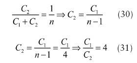
The ratio of C1 to C2 is 4.
The final design step for the 144-MHz oscillator using the largesignalapproach involves finding the value of inductor L, which can be performed by knowing the relationship of the oscillator's operating frequency to the inverse of the square root of the oscillator's inductance and capacitance and selecting a value of L for optimum phase noise.
The component values for the 144-MHz oscillator (C1, C2, C3, C4, and L) can be calculated in the following way. First, the values of capacitors C1 and C2 can be found from the following approach. The value of capacitor C1 is selected for proper loading according to Eq. 32 (see box 1 for equation).
If using a ratio of C1/C2 = 4, then the value of capacitor C2 is approximately 11 pF.
The values for capacitors C3 and C4 can be found by again choosing for optimum phase noise and output power, in which case:
![]()
and the capacitive transformer tapping ratio m (C3/C4) should be greater than 10; therefore, the impedance transformation is greater than 100. Thus, for a value of C3 of 22 pF, the value of C4 is 220 pF. Again one needs to use as many as 10 parallel capacitors or a very low-parasitic one that is capacitive to more then 1 GHz.
4. The value of inductor L can be calculated from Eq. 34 (see box 1 for equation). For f0 = 144 MHz, the value of the inductance L3 can be found from Eq. 35 (see box 1 for equation).
The L/C ratio for the 144-MHz oscillator can be calculated in the following way. The energy stored across the resonator circuit for a given conduction angle and drive level is dependent on the characteristic impedance, and can be found from Eq. 36 (see box 1 for equation).
For optimum phase noise and output power, Z should be greater than 3. For example, the L/C ratio for a good approach is

The same test circuit for the small-signal analysis can now be used with the new large-signal component values applied. Reference 9 shows the phase-noise calculations for a Colpitts oscillator. The calculations can also be used to find the phase noise for the 144-MHz oscillator circuit. Using the Nexxim HB simulator from Ansoft Designer, the simulated phase noise agrees closely with measured data.
According to ref. 9, the individual phase noise contribution can be described by using Eq. 38 (see box 1 for equation), as well as Eqs. 39-42 (see box 2 for equations). The total effect of all the four noise
sources can be expressed as the function shown in Eq. 43 (see box 3 for equation).
where
Kf = the flicker noise constant,
AF = the flicker noise exponent,and

It should be noted that the effect of the loading of the Q of the resonator is calculated by the noise transfer function multiplied with the sum of the four noise sources.
The next step for the 144-MHz oscillator is to compute the phase-noise contribution from the different noise sources for the parallel tuned Colpitts oscillator circuit at a frequency offset of 10 kHz from the oscillator carrier frequency (f0) of 144 MHz. This is performed by considering the circuit parameters. For example, the base resistance (rb of the transistor is 6.14 ohms while the parallel loss resistance of the resonator (RP is 7056 ohms. The Q of the resonator (the Q of the inductor at 144 MHz) is 200, the inductance of the resonator is 39 nH, and the capacitance of the resonator is 22 pF. The transistor collector current (Ic) is 10 mA while the base current of the transistor (Ib) is 85 µA. The device flicker noise component (AF) is 2 while the flicker noise constant (Kf) is 1 ×10⁻⁷. The feedback factor (n) is 5. The phase noise at an offset frequency of 10 kHz for the four noise sources can be found by applying Eqs. 45, 46, 47, and 48 (see the box 4 for equations).
The sum of the four noise sources can be expressed as expressed in the relationship shown as Eq. 49 (shown in box 5).
It should be noted that the noise contribution from the resonator is the limiting factor. For low-Q cases, this can be identified as the flicker corner frequency. When evaluating closer-in phase noise, at an offset of 100 Hz, we have the relationships shown in Eqs. 50 and 51 below:

as well as Eqs. 52 and 53 (shown in the box 4).
The sum of the four noise sources can be expressed by Eq. 54 (shown at the bottom of the box 4).
It appears the collector current, base resistance noise flicker noise from the transistor, and the noise from the resonator are the limiting factors for the overall oscillator phase noise.
Figure 8 and figure 9 show the schematic and layout of the 144 MHz oscillator using time-domain parameters for Ic = 10 mA. The oscillator circuit of Fig. 8 uses a lumped inductor of 39 nH and an unloaded Q of 200 at the operating frequency. The layout is quite critical even at this frequency. The layout in Fig. 8 shows component assembly where lead inductances have been kept small. A standard off-the-shelf inductor was used in the oscillator.
Figure 10, figure 11, and figure 12 show the CAE simulated phase noise plot, the measured phase noise plot, and the simulated output power for the 144-MHz oscillator using the large-signal approach. The simulated and validated output power is +11.55 dBm (a 6-dB improvement over the linear case) and, at 10 kHz offset from the carrier frequency, the phase noise is –135 dBc/Hz, a 13-dB improvement from the value of –122 dBc/Hz for the small-signal, linear approach.
By applying the phase-noise calculation approach used earlier, the phase noise levels for the large-signal 144-MHz oscillator are found to be -134 dBc/Hz offset 10 kHz from the carrier frequency and -94 dBc/Hz offset 100 Hz from the carrier frequency. The calculated, simulated, and measured results all agreed within 1 dB. For designers not having access to expensive CAE tools with the proper oscillator noise-calculation capabilities, this approach with its capabilities of calculating phase noise can be quite useful and cost-effective.
If the same transistor is now run at 30 mA, the phase noise offset 10 kHz from the carrier will improve further to –144 dBc/Hz with the oscillator’s output power increased to +20 dBm at 144 MHz. This demonstrates that choosing a high-output transistor can aid in achieving a low-phase-noise oscillator design. Still, it is important to consider the device’s DC dissipation, since a CAE software tool will not flag a misuse of the device in this way.
A second, higher-frequency, 433-MHz oscillator example may help to further demonstrate the usefulness of the large-signal oscillator design approach. The same transistor (Infineon model BFR193) can be used as in the earlier example, with device parameters of Vce = 8.8 V, Ic =10 mA, IB = pA, and Vbe = 0.67 V. The same set of design equations and conditions at this frequency yield C1 = 3.3 pF, C2 = 13 pF, C3 = 7.5 pF, C4 = 7.5 pF, C3B = 75 pF, LE = 13 nH, RE = 320 ohms, RB1 = 29000 ohms, RB2 = 20000 ohms, CB = 220 pF, Cc = 1000 pF, and VDC = 12 V.
These values result in an output power of +11.9 dBm and phase noise of – 100 dBc/Hz offset 10 kHz from the carrier. The 144-MHz oscillator yielded about 35 dB drop in phase noise (-135 dBc/Hz offset 10 kHz from the carrier), although such a drop-off in phase seems unusual. The phase noise and the carrier frequency are related in a quadratic fashion, so that a three times increase in carrier frequency will result in a 9-dB degradation in phase noise (as shown in Fig. 8 for a comparison of a 432-MHz oscillator with a 144-MHz oscillator). Therefore, the phase noise for a 432-MHz oscillator circuit should be -126 dBc/Hz rather than the CAE-simulated -100 dBc/Hz offset 10 kHz from the carrier for the 433-MHz oscillator. The answer lies in the fact that that even in a grounded-base condition, the large signal Re [Y22] loads the parallel tuned circuit significantly, resulting in a lower dynamic operating Q. This is a limitation that must be overcome.
Because phase noise and Q are related in a quadratic function, a doubling of Q results in a 12-dB improvement in phase noise. Since 26 dB phase noise was lost in the switch to the higher-frequency oscillator design, the dynamic loaded operating Q must be improved by about 20 times the initial value. Since this cannot be done, it may be possible to find effects other than the deterioration in Q that effect the phase noise. One answer is that “ the collector emitter capacitance dynamically detunes the circuit periodically.” A solution for this problem is to tap the inductor, therefore, decreasing the influence of the transistor.
An inspection of the [Y22] parameters for the oscillator transistor at 432 MHz and 30 mA will reveal that loading of the tank circuit decreases the operating Q significantly. The way around this is to apply a center-tapped inductor. As the coupling at these frequencies from winding to winding is not extremely high, two separate identical inductors can be used for this purpose. Figure 13 shows the schematic diagram of the 432-MHz grounded base oscillator using the tapped inductor, a modification of the oscillator circuit used previously. In the case of a VCO, it would be advantageous to use a different outputcoupling scheme since the loading would vary with frequency. This can easily be achieved by adding inductive coupling, such as a printed resonator, to the oscillator circuit.
Figure 14 shows the layout of the 433-MHz oscillator circuit using a buried printed coupled-line resonator network (with a stripline resonator in the middle layer of the circuit board).
The actual resonator would not be visible if performing a visual inspection of the oscillator.
Figure 15 offers a plot of simulated phase noise. It shows the expected noise degradation of 9 dB, since the frequency is approximately three times higher than the earlier example (144 MHz). The resulting simulated output power at 432 MHz is +16 dBm, compared to +18 dBm for the 144-MHz oscillator. This is due to internal package parasitics, which could not be compensated for externally. Second harmonics are suppressed by 38 dB due to the higher operating Q.
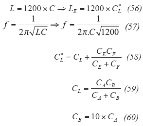
The results obtained so far were based on mathematical calculations, some difficult to obtain. However, by inspecting the resulting circuits, there are certain relationship between the values of the capacitance of the tuned circuit and the two feedback capacitors, the collector emitter capacitor and the emitter to ground capacitor. The following shows the set of recommended steps for easy design of such oscillator. Figure 16 shows the typical grounded base oscillator for demonstrating the simple design rules where CE and CF are the feedback capacitors that generate the negative resistance to compensates the loss resistance of the resonator network comprised of inductor LE and capacitance C*L.
By setting the L/C ratio to a fixed value of 1200 (this is done for optimum energy storage, group delay and energy transfer for a given cycle in the resonator network), the sequence of equations represented by Eq. 55 (see box 6) and Eqs. 57, 58, 59, and 60 below should be used:
The accuracy of this simple approach can be evaluated by applying it to the 144-MHz grounded-base oscillator from Fig. 10 (radio amateurs reading this article will certainly appreciate this oscillator example), using the relationships represented in Eqs. 61-67 shown below:
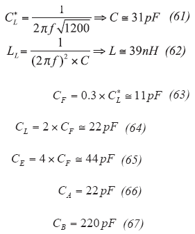
These results are comparable with the results above and the calculation is frequency scalable with minor corrections possibly, if necessary. Competing other alternative short formulae published in the literature may not deliver the same high performance.
Many modern applications require high-performance, low-cost oscillators and design time is critical for realizing these components. The approach shown here meets these requirements and gives detailed guidelines for better-performing oscillators. Several examples have been presented for the approach, but it can be applied to a wide range of different frequencies and oscillators. In addition, the design approach can be readily translated to integrated-circuit designs to achieve extremely small, low-cost oscillators. The equations used in the calculations are fairly simple and provide accurate predictions of phase noise and output power for frequencies to about 200 MHz. At frequencies above about 500 MHz, nonlinear CAE tools should be applied.
Synergy Microwave Corp.
201 McLean Blvd., Paterson, NJ 07504
Phone:(973)
881-8800
FAX: (973) 8818361
E-mail: sales@synergymwave.com,
Internet: www.synergymwave.com
References:
- 1. F. E. Terman , Radio Engineers’ Handbook, McGraw- Hill, New York, 1943, p. 498.
- F. Langford-Smith, Ed., Radiotron Designers Handbook, Electron Tube Division, RCA, Harrison, NJ, 1954, p. 947.
- L. J. Giacoletto, Electronics Designers’ Handbook, McGraw-Hill, New York, 1977, p. 16-1.
- F. Vilbig, Lehrbuch der Hochfrequenztechnik, vol. 2, Akademische Verlagsgesellschaft Becker & Erler Kom.- Ges., 1937/1942, p. 235.
- K. L. Kotzebue and W. J. Parrish, "The Use of Large Signal S-parameters in Microwave Oscillator Design," in Proceedings of the 1975 International Microwave Symposium On Circuits and Systems.
- V. Rizzoli, A. Neri, A. Costanzo, and F. Mastri, "Modern Harmonic-Balance Techniques for Oscillator Analysis and Optimization," in RF and Microwave Oscillator Design, M. Odyniec, Ed. Artech House, Norwood, MA, 2002.
- W. Anzill, F.X. Kaertner, and P. Russer, "Simulation of the Single-Sideband Phase Noise of Oscillators," Second International Workshop of Integrated Nonlinear Microwave and Millimeterwave Circuits, 1992.
- Guillermo Gonzalez, Foundations of Oscillator Circuit Design, Artech House, Norwood, MA, 2007.
- Ulrich L. Rohde, Ajay K. Poddar, and Georg Boeck, The Design of Modern Microwave Oscillator for Wireless Applications Theory and Optimization, Wiley, New York, 2005.
- Kenneth M. Johnson, "Large Signal GaAs MESFET Oscillator Design," IEEE Transactions on Microwave Theory & Techniques, vol. MTT-27, No. 3, March 1979.
- Kenneth. K. Clarke, "Design of Self-Limiting Transistor Sine-Wave Oscillator," Circuit and Systems, IEEE Transaction on [legacy, pre-1988], vol. 13, issue 1, March 1966, pp. 58-63.
- U. L. Rohde and J. Whitaker, Communication Receivers: DSP, Software Radios, and Design, 3rd ed., McGraw- Hill, New York, 2001, pp. 413-422.
- U. L. Rohde and D. P. Newkirk, RF/Microwave Circuit Design For Wireless Applications, Wiley-Interscience, New York, 2000, pp. 798-812, 413-422.
- Moshe Gitterman, The Noisy Oscillator
The First Hundred Years, From Einstein
Until Now, World Scientific Publishing Co., 2005. - M. Tiebout, Low Power VCO Design in
CMOS, Springer Series in Advanced Microelectronics,
Springer, Berlin, 2006. - Edmar Camargo, Design of FET Frequency Multipliers and Harmonic Oscillators,
Artech House, Norwood, MA, 1998. - Randall W. Rhea, Oscillator Design And Computer Simulation, 2nd ed., SciTech Publishing, Raleigh, NC, 2006.
- M. Odyniec, Ed., RF And Microwave Oscillator Design,Artech House, Norwood, MA, 2002.
- Peter Vizmuller, RF Design Guide: Systems, Circuits, and Equations, Artech House, Norwood, MA, 1995.
- U. L. Rohde and A. K. Poddar, "Impact of Device Scaling on Oscillator/VCO Phase Noise in SiGe HBTs," International Semiconductor Device Research Symposium, ISDRS 2005, Dec. 7-9, 2005.
- 21. U. L. Rohde and A. K. Poddar, "Reconfigurable Concurrent
Oscillators For Multi-Band Multi-Mode Wireless Communication Systems," IEEE Sarnoff Symposium, Princeton, NJ, April 30, 2007 to May 2, 2007.
- U. L. Rohde and A. K. Poddar, "Wideband Voltagecontrolled
Oscillators Employing Evanescent Mode Coupled Resonators," United States Patent No. 71803812, February 2007. - U. L. Rohde, A. K. Poddar, and R. Rebel, ;"Integrated Low Noise Microwave Wideband Push- Push VCO",United States Patent No. 7,088189, August 2006.
- U. L. Rohde and A. K. Poddar, "Injection-Tuned Coupled Oscillators," IEEE Radio Wireless Symposium 2008, pp. 367-370, January 22-24, 2008, Orlando, FL.
- U. L. Rohde and A. K. Poddar, "STPCR Offers Integrable Alternatives of DRO," IEEE MTT-S, June 2008, Atlanta, GA.
- U. L. Rohde and A. K. Poddar, "Feedback and Mode-Coupling Improves the Phase Noise Performance of Crystal Oscillators," 2008 IEEE International Frequency Control Symposium, May 18-21, 2008, Honolulu, HI.
- U. L. Rohde and A. K. Poddar,"Mode-Coupled VCO Replaces Expensive DRO, 2008 IEEE International Frequency Control Symp., May 18-21, 2008, Honolulu, HI.
- U. L. Rohde and A. K. Poddar, "User-Definable Thermal Drift Voltage Controlled Oscillator," US Patent No. 7,262,670 B2, August 28, 2007.
- U. L. Rohde and A. K. Poddar, "Low Thermal Drift Tunable Frequency Voltage Controlled Oscillator, US Patent No. 7, 292,113, November 6, 2007.
- U. L. Rohde and A. K. Poddar, "Tunable Oscillator, US Patent No. 7,292,113, November 6, 2007.
- U. L. Rohde and A. K. Poddar, "Tunable Frequency, Low Phase Noise and Low Thermal Drift Oscillator," US Patent No. 7196591, March 2007.
- U. L. Rohde and A. K. Poddar, "Multi-Octave Band Tunable Coupled-Resonator Oscillator," US Patent No. 292,113, November 6, 2007.